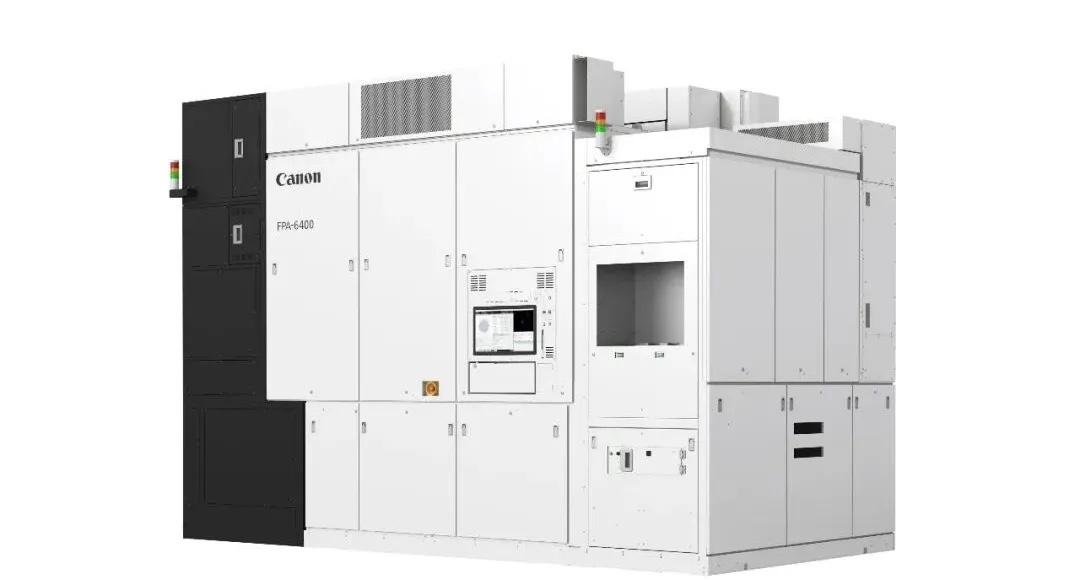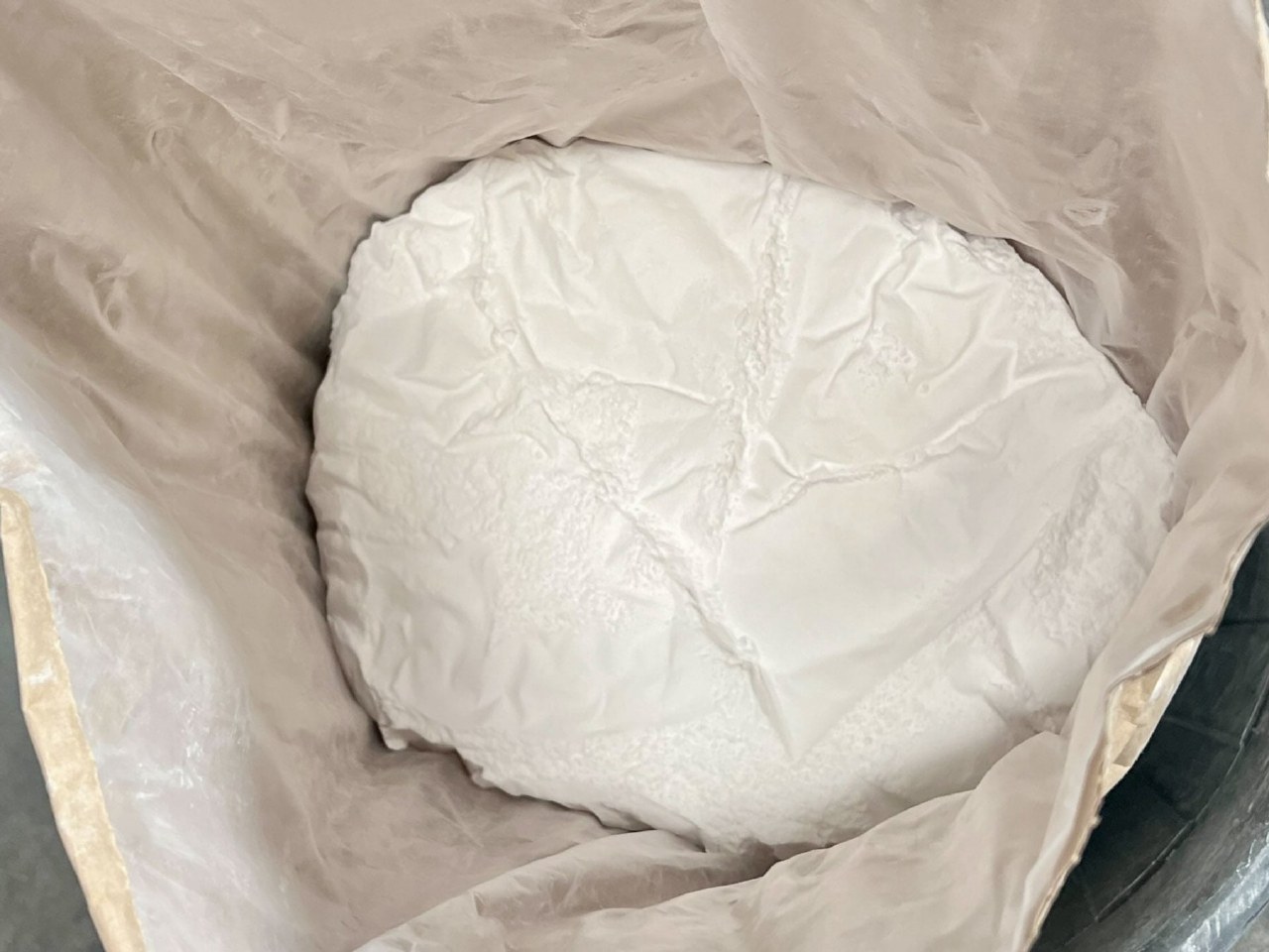


Infineon Technologies has successfully manufactured functional silicon carbide (SiC) chips using 300-millimeter wafers. The testing took place at the company's facility in Villach, Austria, utilizing existing production equipment typically reserved for standard silicon chips. This marks the first demonstration of such a process within a full-scale industrial environment.
The transition to larger 300-millimeter wafers is expected to increase chip yield per wafer by 2.3 times compared to the current 200-millimeter standard. Additionally, the company tested the Cold Split technology at its Dresden plant, which enables more efficient wafer separation from the source crystal with reduced material waste compared to traditional cutting methods.
Infineon plans to continue developing these technologies while coordinating with partners on timelines for mass production. The company will maintain its 200-millimeter wafer production lines alongside these new initiatives. SiC components are currently utilized in electric vehicles, charging infrastructure, energy storage systems, and industrial equipment, with potential future applications in AI data center power supplies.