
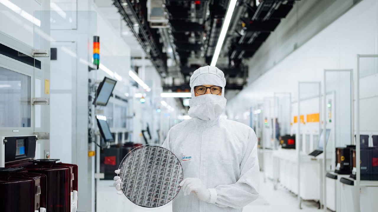
Infineon Technologies has successfully produced silicon carbide (SiC) power semiconductor devices using 300-mm wafers. The pilot production is based at the company's facility in Villach, Austria, where existing equipment for standard silicon chip manufacturing was adapted for the new process.
The transition to 300-mm wafers increases the yield per wafer by 2.3 times compared to the previous 200-mm format. Infineon plans to coordinate the commercial rollout of this technology with partners while maintaining its 200-mm production lines to meet demand in sectors like electric vehicles, charging infrastructure, and AI data centers.
Additionally, the company's Dresden site has validated the Cold Split technology for 300-mm SiC wafers. This method improves material efficiency and reduces processing time compared to traditional wire sawing. Infineon continues to develop silicon, SiC, and gallium nitride (GaN) semiconductors.
In late October, Infineon announced an investment of approximately €1.1 billion to establish mass production of GaN-based power components on 300-mm wafers at its Villach plant.