
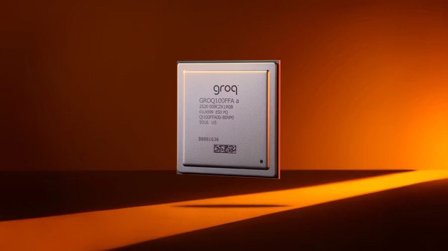
Groq, now part of Nvidia, is shifting its strategy for the next generation of Language Processing Units (LPU). The company plans to replace its current SRAM-based architecture with a 3D-stacked DRAM design. This transition aims to significantly increase memory capacity to support the growing requirements of large-scale artificial intelligence models.
The current generation of Groq LPU chips utilizes 500MB of SRAM, delivering a memory bandwidth of 150TB/s. A single chip provides approximately 1.20 PFLOPs of FP8 computing power. In the LPX rack configuration, which entered mass production in August, 256 chips provide a total of 128GB of SRAM and 640TB/s of bandwidth, achieving speeds of 3400 tokens per second when paired with NVL72 servers.
By adopting 3D stacking and Through-Silicon Via (TSV) technology, Groq intends to stack multiple layers of DRAM vertically. This approach mirrors the structure of High Bandwidth Memory (HBM), allowing for higher storage density and improved energy efficiency. While DRAM offers lower speeds compared to SRAM, it is better suited for building large-scale storage systems.
Groq may continue to develop SRAM and DRAM product lines in parallel to address different use cases. For Nvidia, which is currently building out its AI factory and platform ecosystem, these high-capacity inference chips are expected to play a critical role in future infrastructure deployments.