
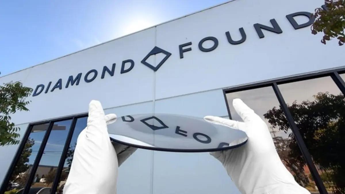
Diamond Foundry has successfully grown the world's first 200 mm single-crystal diamond. This achievement follows 25 years of research into large-scale crystal production. The material was created in the United States using chemical vapor deposition, a process where carbon-containing gas decomposes in controlled plasma to form a structure with precise atomic alignment.
The resulting disk lacks grain boundaries, which typically hinder thermal and electrical conductivity. Pure single-crystal diamond exhibits thermal conductivity of approximately 2000 W/mK at room temperature, significantly outperforming copper. This property is essential for managing heat in high-density AI and computing systems, where diamond substrates could serve as effective heat sinks.
The current specimen remains in an unpolished, raw state. Key metrics such as production costs, scalability, and suitability for mass manufacturing are not yet determined. Future development requires achieving uniform thickness, surface smoothness, and consistent electrical properties. Additionally, engineers must solve challenges related to controlled doping for integration with silicon-based technologies.
The company views the 200 mm milestone as a precursor to developing 300 mm disks, though specific timelines remain undisclosed. To scale production, Diamond Foundry is planning a facility in Spain valued at $2,77 billion, supported by the European Chips Act. The initiative aims to transition diamond from a niche product to a mainstream semiconductor material for high-power and high-frequency applications.