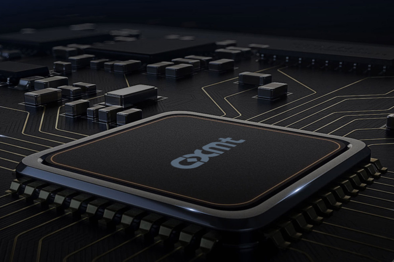
CXMT has started trial production of HBM3E memory stacks, but faces significant yield challenges. The current yield rate is below 25%, far from the 80% industry standard for mass production. In contrast, SK hynix has achieved a 90% yield rate for its HBM3 and HBM3E products.
The primary cause of low yields is the struggle to master Through-Silicon Via (TSV) technology. For 8-layer HBM3E, the front-end yield is approximately 30%, and only 70% of those chips pass the back-end stage. This means nearly 80% of units fail final testing.
CXMT's HBM3E crystals have about 3,000 TSV connections per crystal, compared to over 8,000 in SK hynix's HBM3 and over 5,000 in Samsung's HBM2. To reduce production complexity, CXMT reduced the number of connections, which lowered thethroughput. Throughput is a key performance metric for memory stacks.
The company is supplying small batches of HBM3E samples to Chinese firms, including Cambricon and T-Head (part of Alibaba). While CXMT produces standard DRAM using the G4 process (17nm class), its HBM-specific DRAM crystals require higher surface area and stricter technical specifications, making quality control more difficult.
The company faces difficulties in the back-end process, including mechanical alignment of crystals and their connection. Any shift in alignment or air bubbles during thermocompression can lead to the failure of the entire multi-layer structure. Experts suggest that stabilizing TSV technology requires years of experience.