
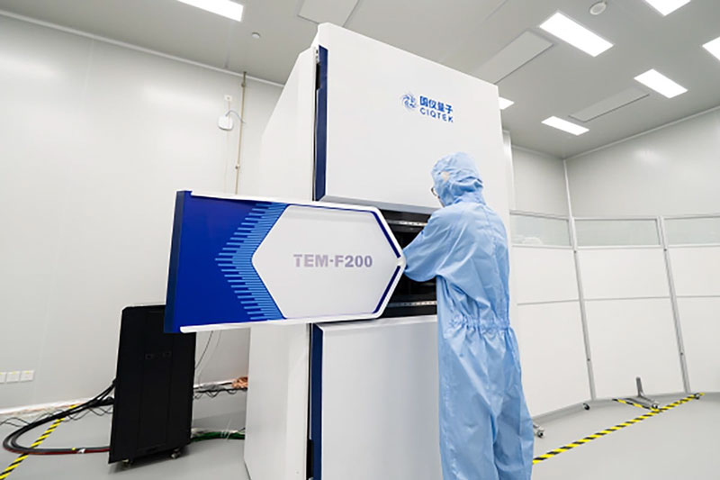
Chinese company CIQTEK has unveiled the TEM-F200, a transmission electron microscope designed for semiconductor analysis. The device operates at an accelerating voltage of 200 kV and achieves a point resolution of 0.25 nm, with a digital resolution limit of 0.1 nm.
The microscope is intended for examining crystal structures, layer boundaries, and manufacturing defects in microchips. CIQTEK states that it developed the key modules, control software, and integration systems in-house. The product is now ready for mass production and commercial delivery.
China is actively developing its own scientific equipment to reduce reliance on foreign imports. Other domestic milestones include the 2024 launch of the TH-F120 model by Bioland Laboratory and the 2025 introduction of the BZ-F200 by Suzhou Bozhon Instrument Technology.
The industry landscape also includes AI-driven solutions, such as the Aeye-1 platform announced by the Chinese Academy of Sciences in May 2026. Globally, the highest point resolution standards are currently set by Thermo Fisher Scientific, JEOL, and Hitachi.