

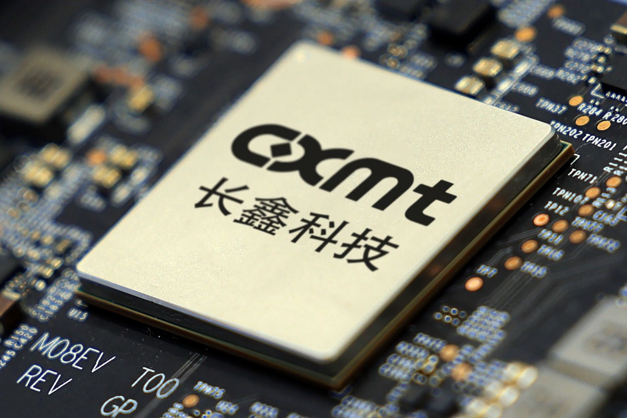
According to South Korean court documents, the Chinese chipmaker CXMT allegedly utilized a detailed roadmap known as Project Hefei to misappropriate Samsung DRAM technology. The plan, initiated around August 2016, aimed to secure a 620-step process recipe, poach key engineers, and reach a monthly production capacity of 10,000 wafers by August 2018.
The prosecution alleges that CXMT lacked internal R&D facilities upon its founding in June 2016. By leveraging stolen data, the company reportedly accelerated its development timeline, eventually capturing approximately 10% of the global DRAM market by Q2 2025. This growth challenged the dominance of the industry's Big Three, which saw their combined market share drop below 90%.
CXMT currently operates three 12-inch wafer fabrication facilities with a collective output of 350,000 wafers per month. The company plans to open a new fab in Beijing to increase capacity to over 600,000 wafers monthly. In July 2026, the firm completed an IPO on the Shanghai STAR Market, raising $8.6 billion and seeing its stock value climb 466%.
Financial reports indicate that CXMT's revenue grew 716% in Q2 2026. The company intends to allocate 70% of its IPO proceeds toward further DRAM production expansion. Meanwhile, South Korean prosecutors estimate that damages to Samsung resulting from the alleged intellectual property theft have reached at least $29.5 billion.